Overview
Verilog is a hardware description language (HDL) used to model, simulate, and implement digital circuits.
Unlike software languages (which describe step-by-step execution), Verilog describes hardware structure and behavior that can run in parallel.
Typical use cases:
- Designing combinational logic (adders, multiplexers, decoders)
- Designing sequential logic (registers, counters, finite-state machines)
- Writing testbenches for simulation and Verification
- Implementing digital designs on FPGA or ASIC flows
Core Ideas
module: the basic building block (like a component with inputs/outputs)wire: signal for combinational connectionsreg: variable-like storage used in procedural blocksassign: continuous assignment for combinational logicalwaysblock, see Always block:always @(*)for combinational behavioralways @(posedge clk)for clocked sequential behavior
Concurrency vs. Software Thinking
Multiple Verilog statements can represent hardware that works at the same time.
So Verilog code should be read as circuit behavior, not as a single-threaded program.
Basic Example
module and_gate (
    input  wire a,
    input  wire b,
    output wire y
);
    assign y = a & b;
endmodule
For number literal syntax (like 2'b11, bases, x/z, and sizing), see Number Representation in Verilog.
Design Flow
- Write RTL (register-transfer level) in Verilog
- Simulate with testbenches to verify functionality (see Verification)
- Synthesize RTL into gates
- Implement/place-route on target technology
- Validate timing and power (see Timing and Power Consumption)
Design Methodologies
- Top-down design: Start from system-level behavior, split into smaller modules step by step, then implement each module in Verilog.
Good for managing complexity and keeping architecture consistent. - Bottom-up design: Start from small reusable building blocks (gates, adders, registers), verify them, then compose larger modules and finally the full system.
Good for reuse and for designs built from well-tested IP blocks.
In practice, real projects often combine both: top-down planning with bottom-up implementation of reusable components.
Structural HDL Example
This style builds a larger design by instantiating submodules and wiring signals between them.
module top (A, SEL, C, Y);
    input  A, SEL, C;
    output Y;
    wire   n1;

    // short (positional) form: pin order must match module declaration
    small i_first (A, SEL, n1);

    // named form: safer, pin order does not matter
    small i_second (
        .B(C),
        .Y(Y),
        .A(n1)
    );
endmodule

module small (A, B, Y);
    input  A;
    input  B;
    output Y;

    // description of small
endmodule
i_first uses positional mapping, so small (A, B, Y) order is critical.
i_second uses named mapping (.pin(signal)), which is usually safer in larger designs.
Behavioral HDL Example
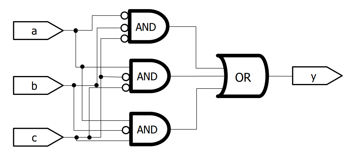
This style describes the logic behavior directly with Boolean expressions.
module example (a, b, c, y);
    input  a;
    input  b;
    input  c;
    output y;

    // here comes the circuit description
    assign y = ~a & ~b & ~c |
               a & ~b & ~c |
               a & ~b &  c;
endmodule
The output y is defined by a sum-of-products style expression using assign.